
The Growing Chasm Between Compute and Memory
The artificial intelligence revolution is facing an unexpected adversary: physics. As large language models grow exponentially—doubling in parameter count every 24 months—memory bandwidth improves at a meager 1.6× over the same period, while floating-point performance increases only 3× . This widening gap between computational capability and data transfer speed represents the memory wall, the single greatest obstacle to AI performance scaling.
Consider the numbers: executing a modern LLM requires moving hundreds of gigabytes of weights and activations between memory and compute units. In conventional von Neumann architectures, data must travel across bandwidth-limited interfaces, consuming up to three orders of magnitude more energy than the computations themselves . For every floating-point operation performed, the system spends exponentially more energy shuffling data—an unsustainable equation as models push toward trillion-parameter scales.
HBM3e: Pushing Against Physical Limits
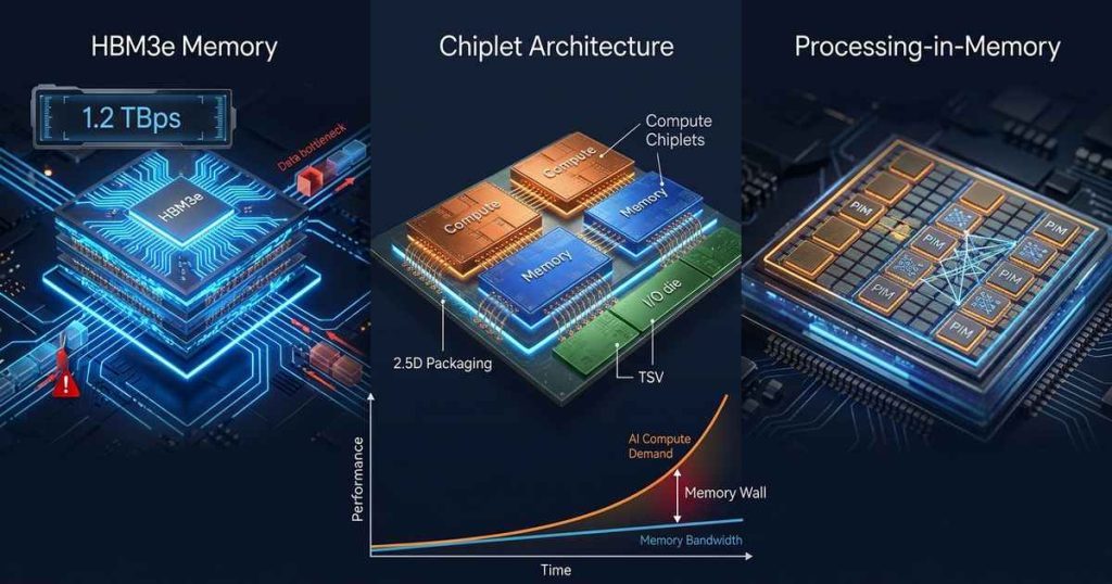
High Bandwidth Memory has emerged as the semiconductor industry’s answer to AI’s insatiable bandwidth demands. The latest HBM3e standard represents the pinnacle of this approach, with companies like Alphawave Semi demonstrating complete HBM3e subsystems achieving 1.2 Terabytes per second (TBps) of bandwidth through advanced 2.5D packaging . Working with Micron’s HBM3e memory, these platforms deliver 9.2 Gbps per pin while maintaining signal integrity across silicon interposers—a remarkable engineering achievement.
Yet HBM3e’s very success reveals the memory wall’s true nature. Each HBM3e stack consumes over 30 watts, making it impractical for edge deployments and creating thermal challenges even in data center environments . More critically, bandwidth improvements are slowing as we approach the physical limits of through-silicon vias (TSVs) and interconnect density. The industry finds itself at a crossroads: continue refining conventional architectures with diminishing returns, or fundamentally rethink how memory and compute interact.
The Geopolitical Dimension: HBM Under Export Controls
The memory wall isn’t purely technical—geopolitics now shapes the landscape. Recent US export controls targeting HBM bandwidth have created significant challenges for AI chip development. Regulations now restrict not only HBM itself but also aggregate memory bandwidth and interconnect speeds, effectively limiting access to HBM3e and HBM3 for affected regions .
These restrictions have accelerated interest in alternative approaches. Chinese AI chip manufacturers are exploring Chiplet packaging technologies alongside GDDR6 and LPDDR5 substitutions to reduce dependence on advanced HBM . Some are reducing HBM count or interface width to comply with bandwidth caps, while simultaneously accelerating domestic HBM development. The message is clear: reliance on monolithic, cutting-edge memory architectures creates strategic vulnerabilities.
Chiplet Architecture: Composable AI Systems
Chiplet-based design represents perhaps the most immediate practical response to the memory wall. Rather than fabricating massive monolithic dies, chiplet architectures decompose systems into smaller, specialized components—compute chiplets, memory chiplets, I/O dies—that integrate via advanced packaging .
The University of Minnesota’s CLAIRE (Composable Chiplet Libraries for AI Inference) project demonstrates the potential of this approach. By developing hardened IP and chiplet libraries optimized for diverse AI applications, researchers achieved 1.99× to 3.99× improvements in non-recurring engineering costs while maintaining performance comparable to custom ASIC designs . The key insight: composable, scalable, and reusable chiplet configurations can accommodate different computing primitives and data volumes without requiring bespoke designs for every application.
Arm’s Compute Subsystems (CSS) and Chiplet System Architecture (CSA) are industrializing this vision. CSS provides pre-validated IP building blocks—cores, accelerators, memory subsystems—while CSA establishes open standards for chiplet interconnect and communication . Together, they enable silicon providers to build AI-optimized chips with performance comparable to hyperscaler designs, but with lower risk and faster time-to-market. Open standards through the Open Compute Project (OCP) further promise supply chain flexibility, allowing dies from multiple foundries to interoperate reliably .
Research institutions are pushing even further. ETH Zurich and the University of Bologna have outlined a roadmap for open-source chiplet-based RISC-V systems targeting HPC and AI, starting with Occamy (a silicon-proven dual-chiplet manycore) and progressing to quad-chiplet concept architectures achieving state-of-the-art compute density .
Processing-in-Memory: Computing Where Data Lives
While chiplets improve system integration, Processing-in-Memory (PIM) attacks the memory wall at its root: eliminating data movement entirely. PIM integrates computational capabilities directly within memory arrays, transforming memory from passive storage into active compute participants .
The PIM Taxonomy
PIM architectures span a spectrum of integration levels :
Processing-Near-Memory (PNM) places compute logic adjacent to memory arrays. Samsung’s AXDIMM exemplifies this approach, integrating AI engines into DIMM buffer chips for parallel processing across multiple ranks. PNM offers easier manufacturability and broader compatibility, though bandwidth remains constrained by interface limitations.
Processing-in-Memory (PIM) proper embeds computational units within the memory chip itself. Samsung’s HBM-PIM integrates SIMD units into HBM2 dies, demonstrating 2.5× system performance improvements with over 60% energy reduction . SK hynix’s GDDR6-AiM embeds 16 processing units per DRAM die, supporting BF16 precision for AI workloads .
In-Array Computing pushes integration to the ultimate level, performing operations directly within memory arrays using analog or digital techniques. The NSF-supported CIDAN-3D architecture exemplifies this approach, introducing configurable neuron processing elements that interface with each DRAM bank’s row buffers . By implementing threshold functions rather than conventional CMOS logic, CIDAN-3D achieves exceptional compute density—a carry-out function in the area of a single D-flipflop at 40nm. The architecture delivers 21.55× average throughput improvement over GPUs and up to 71× energy efficiency gains for decoder-only models .
Commercial PIM Implementations
Industry leaders are actively commercializing PIM. Samsung offers a portfolio spanning HBM-PIM for data centers, LPDDR5-PIM for mobile devices, and AXDIMM for memory database workloads . SK hynix focuses on AI acceleration with GDDR6-AiM and the AiMX PCIe accelerator card .
Most significantly, Qualcomm’s 2025 acquisition of UPMEM—the first company to commercialize programmable PIM—signals mainstream validation. UPMEM embeds hundreds of 32-bit RISC processors (Data Processing Units) directly into DDR4 DIMMs, complete with software development kits that make PIM programmable rather than application-specific .
The PIM Software Challenge
Hardware advances alone cannot breach the memory wall. PIM introduces fundamental software challenges: how to program distributed compute elements embedded within memory, how to manage data layout for optimal locality, and how to integrate PIM operations with conventional CPU instruction flows .
Current approaches divide into two paradigms : MMIO-based asynchronous programming offers flexibility and independent PIM core programming but requires complex software stacks. CPU instruction set extension provides better ecosystem compatibility but faces instruction bandwidth and bus contention challenges. CIDAN-3D addresses this through explicit CPU ISA extensions and memory controller modifications, enabling optimized dataflow for transformer model kernels .
Edge AI: Different Constraints, Same Problem
The memory wall manifests differently at the edge, where power constraints dominate. Winbond’s CUBE platform targets this domain with custom DRAM solutions optimized for AI workloads. CUBE-Lite delivers 8-16 GB/s bandwidth at just 30% of LPDDR4x power, enabling AI acceleration in battery-powered devices without HBM’s 30W thermal footprint .
For TinyML applications, integrating PIM-capable DRAM with NPUs or AI MCUs creates new possibilities. IP cameras, AI glasses, and wearables can run AI-ISP workloads with dramatically improved efficiency by minimizing data movement between memory and processing elements .
The Road Ahead: Heterogeneous Memory Hierarchies
The memory wall won’t be solved by any single technology. The future belongs to heterogeneous memory hierarchies that combine multiple approaches :
- HBM3e and beyond for highest-bandwidth near-compute memory
- PIM-enhanced DRAM for memory-bound workloads like GEMV operations
- Chiplet-based integration for flexible, scalable system composition
- CXL-attached memory for capacity expansion with cache coherence
- AI-optimized DRAM like CUBE for edge deployments
As DDR6 targets 200+ GB/s module bandwidth and HBM4 pushes beyond today’s limits, the fundamental truth remains: moving data costs far more than computing on it. The memory wall persists because physics favors locality. Processing-in-memory and chiplet architectures don’t just incrementally improve performance—they align computation with this physical reality.
Conclusion
The memory wall represents AI’s most fundamental hardware challenge. HBM3e’s 1.2 TBps bandwidth, while remarkable, only temporarily forestalls the inevitable: we must bring computation to data, not the reverse. Chiplet architectures enable flexible, composable systems that optimize the compute-memory balance. Processing-in-memory technologies—from Samsung’s HBM-PIM to UPMEM’s programmable DIMMs—reimagine memory as an active computing layer.
The winning AI hardware platforms will be those that most effectively minimize data movement, whether through 3D stacking, chiplet integration, or in-memory computation. The memory wall isn’t going away—but neither are the innovators determined to breach it.